

Hello! This is Linkgenesis 🙂
Today we’d like to talk about something that’s been getting a lot of attention on semiconductor and display lines lately: deep-learning-based machine vision inspection.
A single wafer carries tens of billions of microscopic circuit features, and just one defect — a few thousandths the width of a human hair — can turn an entire chip into scrap.
So how on earth do we catch defects that small and that varied?
What Was Missing in Traditional Vision Inspection?
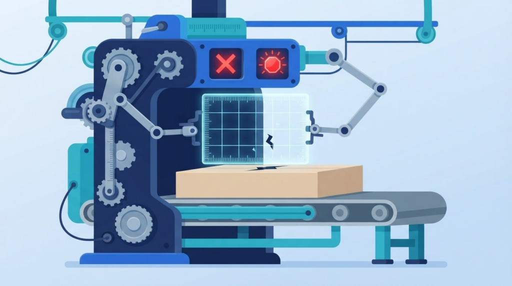
Classic machine vision is rule-based.
An engineer defines the criteria by hand — “flag anything darker than this threshold,” for example.
It works beautifully for simple, stable products, but the moment a defect changes shape or a brand-new failure mode appears, the rules have to be rewritten.
Subtle, irregular, or never-before-seen defects are especially hard to pin down with fixed rules.
So what makes deep learning different?
Instead of hand-coding the criteria, you train a model on images of good and defective parts, and it learns to recognize “what normal looks like” and flag deviations on its own.
Recent industry reporting shows AI catching residual tungsten defects at wafer edges that traditional methods missed entirely, and X-ray tools classifying solder-bump voids in milliseconds with around 90% accuracy.
In 2026, the Real Challenge Is Data

But AI inspection is no silver bullet.
The bottleneck the industry keeps pointing to in 2026 isn’t the algorithm — it’s data.
By one account, more than 70% of AI inspection projects stall after the pilot stage, undone by fragmented data, legacy systems, and imbalanced datasets. Most factories have far more images of good units than defective ones, so the models lack the very defect examples they most need to learn from.
The response has been twofold: synthetic data, which artificially generates rare defect images for training, and hybrid pipelines that pair deep learning with proven rule-based checks.
The pull is broad — the global machine vision camera market is projected to reach roughly $10.1 billion by 2030, as AI-powered, high-resolution inspection spreads across semiconductor, EV battery, and logistics applications.
How Linkgenesis Approaches It

In step with this shift, Linkgenesis offers VLAD (Vision Learning for Advanced Detection), our deep-learning image-analysis solution for industrial surface inspection.
VLAD bundles a training tool, report viewer, and testing tool so that building and validating an inspection model happens in one connected workflow.
And through VLAD Ops, it extends into full MLOps — data labeling → modeling → deployment → monitoring — so the “data bottleneck” we described above can actually be managed in production instead of derailing a pilot.
Wrapping Up
Deep learning machine vision moves past the limits of hand-written rules, learning to catch subtle and novel defects. But the decisive battleground in 2026 is data quality and MLOps, not the algorithm itself. The winning move is a virtuous loop: detect → train → deploy → retrain.
Is your line wrestling with defects that rule-based tools can’t catch, constant re-tuning every time a new failure mode appears, or inspection images that just pile up unused?
Our VLAD solution connects deep-learning model training, deployment, and monitoring end to end, lifting detection accuracy and operational efficiency together.
You can always reach us through the Linkgenesis website for a consultation or any questions — we’d be glad to help map the right AI inspection strategy for your process 🙂
Thank you for visiting our blog again today. Have a great day!
